FPGA Neural Network Accelerator
In the context of neural network inference on embedded systems, overall performance is usually poor because of the limited resources available: small amount of ROM, RAM, low MCU frequency. This limits both the complexity of the model - and with it the amount of ‘things’ the system can recognize - as well as the ability to perform such recognition quickly. To overcome these limitations, multiple methods are available. First the model can be quantized from float to an integer only model (typically int8 quantize). This makes the computation a lot faster on MCU without requiring FPU support. Additionally, some micro-controller architecture provides their own software libraries for optimized (vectorized) computation. Lastly, hardware accelerators (TPU) which are generic and adapt to any model. Most of the time these accelerators are configured via software and then executed one layer at a time.
As an alternative we implemented our own FPGA based neural network accelerator. This accelerator is highly specialized and generated specifically for a given model. Changing the model will require rebuilding a new gateware.
Overview
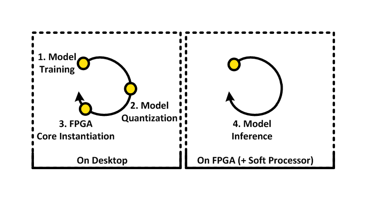
1. Model training
The model is first designed and trained on a desktop environment with TensorFlow, where we can benefit from the GPU acceleration during the learning phase.
2. Model quantization
Once the model is trained, it is quantized to int8 (Post-training quantization) and exported to a TensorFlow Lite model (.tflite file) using the TFLite converter.
3. FPGA core instantiation
The model file is then fed into our framework:
- The model file is parsed with FlatBuffers to extract the layer types and parameters.
- Supported layers are automatically generated as FPGA cores: each layer gets its own specific core. The parameters like shapes, weights, bias, etc. are embedded in each core ROM.
- Non supported layers will fallback to the standard TensorFlow Lite Micro software implementation.
- The FPGA SoC is compiled, it contains a RISC-V soft processor that will run TensorFlow Lite Micro, and the layer accelerator cores mapped as peripherals within the SoC address space.
4. Model inference
The bitstream is loaded on the FPGA and runs the model in a infinite loop.
Use-case: sound recognition
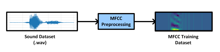
We would like to recognize spoken numbers from 0 to 9. For this we use a subset of the TensorFlow Speech Commands Datasets. For a better representation of sound and thus better model accuracy we have first preprocessed the dataset .wav files through our MFCC core (Mel-frequency cepstral coefficients), and use the output coefficients for training the model.
1Number of total examples: 23666
2Number of labels: 10
3Training set size: 18932
4Validation set size: 2367
5Test set size: 2367
6Input shape: (1488,)
Model description
We created a very simple model with 2 convolution layers and 1 dense layer as follows (where the number of kernels and their size have been optimized with hyper parameter tuning):
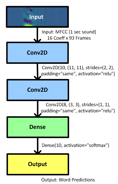
We also truncated the MFCC input originally containing 32 coefficients to keep only the 16 lower coefficients which are the most significant for word recognition, the other ones carrying other information like emotion which are no use to us in this case. This truncation reduces the model size by 2 without impacting the accuracy !
This allows both to keep the model within a reasonable size (~30k) and to retain a decent accuracy (~89%).
1Trainable params: 29,029
2Test set accuracy: 89%
Once trained the model is converted to TensorFlow Lite: as we can see on the conversion output below, model quantization from float to int8 has a very negligible impact on accuracy (-0.04 % accuracy loss).
1Float model accuracy is 89.0579% (Number of test samples=2367)
1Quantized model accuracy is 89.0156% (Number of test samples=2367)
2input_details quantization: (scale: 77.17254638671875, zero point: -72)
3output_details quantization: (scale: 0.00390625, zero point: -128)
Development setup
For development with use the ECPIX-5 85F board, with a PMOD Sipeed I2S Mic for sound acquisition and a PMOD 7-Segment Display for showing the inference result.
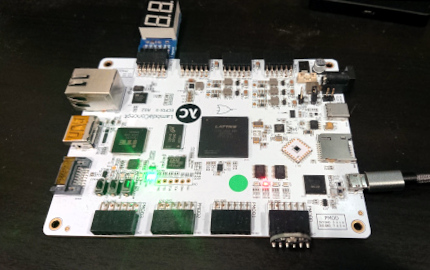
On this platform we are running NuttX RTOS on our Minerva 32-bit RISC-V soft processor. The whole environment is based on nMigen and compiled with Yosys+nextpnr.
Timing analysis
When running the model inference without any hardware acceleration, only with the TFLite Micro software reference implementation, each inference takes ~3.4 seconds to complete (SoC system clock 70MHz), which is too slow for detecting words contained in a 1 second timeframe.
We thus want to offload some of the computation to an accelerator core, and we begin with the layer that requires the biggest amount of operations. We can pull the following estimation on the number of multiplication operations per layer:
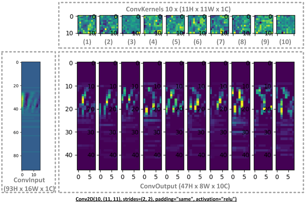
- Conv2D(10, (11, 11), strides=(2, 2), padding=“same”, activation=“relu”)
 1Kernel shape: 11 Height x 11 Width:
 2	Each convolution with one kernel at a given position yields 121 multiplications.
 3
 4Input shape: 93 Height x 16 Width x 1 input Channel.
 5Due to strides (2, 2), padding "same", and 10 kernels:
 6	Output shape: 47 Height x 8 Width x 10 output Channels = 3760.
 7
 8Thus we have 121 x 3760 = 455 kMuls for a full convolution.
 9We also count the per channel quantifier multiplications that are done on the output shape: 3760.
10
11We get 459 kMuls for the first convolution layer.
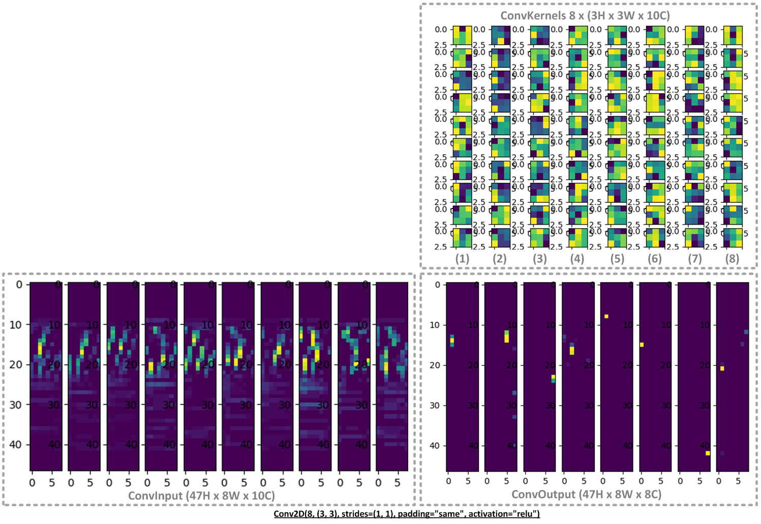
- Conv2D(8, (3, 3), strides=(1, 1), padding=“same”, activation=“relu”)
1With a similar calculus, we get:
2
3Kernel: 3 Height x 3 Width x 10 input Channels:
4	90 multiplications per kernel.
5
6Output shape: 47 Height x 8 Width x 8 output Channels = 3008.
7
8We get 90 x 3008 + 3008 quantifier multiplications:
9	273 kMuls for the second convolution layer.
- Dense(10, activation=“softmax”)
1This is a matrix multiplication: 3008 x 10 = 30 kMuls
Also because we use a int8 quantized model, but our MFCC input is still 16bits wide we have to perform a quantization input scaling before each model invocation with the formula:
1quantized_input = raw_input / input_scale + input_zero_point
2Input shape:  93 x 16 x 1 input channel = 1488 divisions.
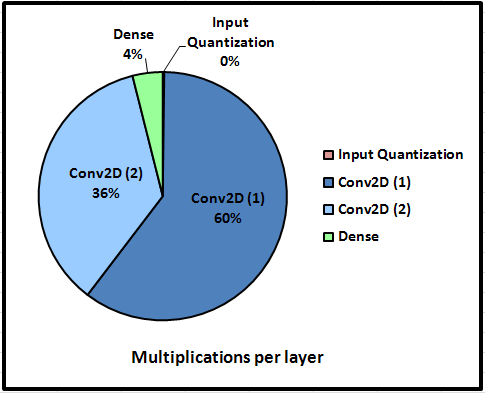
Let’s focus on the two convolution layers which take about 96% of the computation time.
SoC overview
We plan to develop an accelerator core for the convolution and add it the FPGA SoC as shown below:
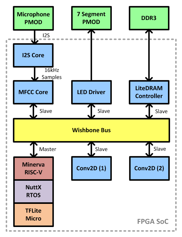
The microphone captures the sound at 16 kHz and streams it via I2S to the MFCC converter. This happens continuously on the FPGA without requiring any CPU time. The resulting MFCC buffer is exposed on the bus so the CPU can fetch it. The NuttX application we developed first quantizes the MFCC coefficients using the scale and zero point values, fills the TensorFlow Lite Micro Interpreter buffer and invokes the model inference. Once the inference is complete, the result of the word prediction is displayed on the 7 segment module for visual feedback.
Integration with TensorFlow
Within TensorFlow, our convolution accelerator is handled as an optimized kernel layer (compiled with OPTIMIZED_KERNEL_DIR=). Whenever TensorFlow will need to perform a convolution, it will call our FPGA accelerator instead of using the software reference implementation.
FPGA convolution core
This is our convolution core, two of them will be instantiated in the FPGA (with different sizes and parameters, one for each convolution layer):
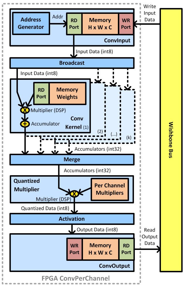
-
ConvInput: This module contains a memory buffer for storing the convolution input data. Size of the input memory: H x W x C, arranged in ‘channels_last’ format. Typically it will be initialized with input data coming from the application logic through the write port exposed on the Wishbone bus.
-
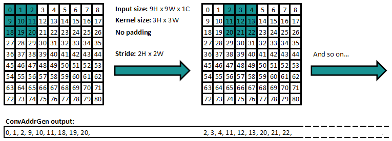
ConvAddrGen: This modules computes the addresses required to fetch the input data from the memory buffer, and streams the addresses on the source stream. It takes into account the input size, number of channels, kernel sizes, strides, padding, dilation, etc.
The address generator module is the most complicated one, to understand why, we need to look at how a convolution operation is made. Explaining the convolution itself is beyond the topic of this article, so let’s refer to this very good visual explanation: https://towardsdatascience.com/conv2d-to-finally-understand-what-happens-in-the-forward-pass-1bbaafb0b148
For example, for a input size 9 x 9, kernel size 3 x 3, stride 2 x 2, no padding, the module will generate the following addresses:
-
Broadcast: This module simply duplicates the input data stream into multiple identical streams. This will ease interconnection with convolution kernel modules, each receiving its own input data stream.
-
ConvKernel: This module performs a convolution operation (sum of products). Each multiplication product is computed using an input value from the sink stream (minus the zero point offset) and a weight stored in the internal memory bank. The weights are taken from the model file at build time and each kernel is provided with its own read only weights (H x W x C). All multiplication results are accumulated (summed) and the result (plus bias) is sent out on the source stream (int32).
-
Merge: This module takes the accumulated data streams coming separately from all the kernel modules and aggregates them into one stream in a round robin fashion. This will ease interconnection with the next modules.
-
QuantizedMultiplier: This module re-quantize the accumulator data int32 into int8. For this it performs on each output channel a saturating rounding multiplication operation with coefficients taken from the model file. Basically this is a hardware implementation of this function: https://github.com/tensorflow/tensorflow/blob/master/tensorflow/lite/kernels/internal/common.h#L156
-
Activation: Very simple activation layer module: the output data less than the minimum (resp. greater than the maximum) activation value is clamped.
-
ConvOutput: This module contains a memory buffer for storing the convolution output data. Size of the output memory: H x W x C, arranged in ‘channels_last’ format. Typically it will be read from the application logic through the read port exposed on the Wishbone bus, once the convolution is completed (signaled with interrupt and status register).
Simulation
We can benefit from the nMigen simulator (pysim) to unittest each of our submodules. For testing with realistic data, the simulator will be fed with intermediate tensors obtained with the experimental TensorFlow Lite feature “preserve_all_tensors”. This way we can make sure the output from our cores matches the reference output from TensorFlow, layer by layer. And we can visualize the result with matplotlib, very handy for debugging ! Also the simulator generates a .vcd file for deeper inspection with GTKWave.
1# Initialize the interpreter
2interpreter = tf.lite.Interpreter(model_path="model.tflite",
3                                  experimental_preserve_all_tensors=True) # pip install tf-nightly
4interpreter.allocate_tensors()
And later (example with tensors for Conv2D (1)):
 1tensors = {
 2	"din": 10,
 3	"kernels": 4,
 4	"bias": 5,
 5	"dout": 11,
 6}
 7
 8# Get tensors
 9din     = interpreter.get_tensor(tensors["din"])
10kernels = interpreter.get_tensor(tensors["kernels"])
11bias    = interpreter.get_tensor(tensors["bias"])
12dout    = interpreter.get_tensor(tensors["dout"])
This is how it looks with “dataset/one/c37a72d3_nohash_0.mfcc”:
Simulator output for Conv2D (1):
 1$ time python -m unittest ai.layers.tests.test_conv
 2ishape: (93, 16)
 3kshape: (11, 11)
 4oshape: (47, 8)
 5nkernels: 10
 6nchannels: 1
 7strides: (2, 2)
 8dilation_rate: (1, 1)
 9zero points: -72 -128
10per_channel_multshifts: [(1293535282, -6), (1214362513, -6), (1144390327, -5), (1435400891, -6), (1631131071, -6), (1789671352, -6), (1421322341, -6), (1445871427, -6), (1867516801, -6), (1678316352, -6)]
11activation min max: -128 127
12mem_width: 32, mem_size: 3760: mem_depth: 940
13
14cycles: 45509
15validate: nerrors: 0
Likewise, we can run the simulation for the second convolution layer. This time the input data is in fact the output data from the previous convolution layer:
Simulator output for Conv2D (2):
 1$ time python -m unittest ai.layers.tests.test_conv
 2ishape: (47, 8)
 3kshape: (3, 3)
 4oshape: (47, 8)
 5nkernels: 8
 6nchannels: 10
 7strides: (1, 1)
 8dilation_rate: (1, 1)
 9zero points: -128 -128
10per_channel_multshifts: [(1221539373, -4), (1855100688, -5), (1333592641, -5), (1649548783, -5), (1393609797, -4), (1391918024, -4), (1479537844, -4), (1753616432, -5)]
11activation min max: -128 127
12mem_width: 32, mem_size: 3008: mem_depth: 752
13
14cycles: 33852
15validate: nerrors: 0
Resource consumption
Now that the convolution core is functional in simulation we can compile it for a real FPGA. For doing the multiplication operation contained in the convolution and in the requantization, we use the multiplier blocks present on the FPGA fabric. On Lattice ECP5 they are called MULT18X18D as they can perform a 18bits x 18bits multiplication at each clock cycle.
- Convolution multiplication:
1op1: input data (int8)
2op2: kernel weight (int8)
These multiplications fit in one MULT18X18D. Each kernel allocates its own multiplier block so they can all work in parallel.
Cost in term of resources:
1Conv2D (1): 10 kernels
2Conv2D (2): 8 kernels
310 + 8 = 18 MULT18X18D
- Requantization multiplication:
1op1: convolution accumulator (int32)
2op2: per channel multiplier (int32)
The operands cannot fit in 18 bits this time, therefore we need 2 MULT18X18D blocks for each operand, 4 in total. Fortunately this operation can occur after the Merge block, see above, so they can be shared between all the kernels in the same convolution layer.
1Conv2D (1): 4
2Conv2D (2): 4
34 + 4 = 8 MULT18X18D
On ECPIX-5 board LFE5UM5G-85F for the entire SoC including Minerva RISC-V + LiteDRAM + MFCC core + 2 Convolution cores:
 1Info: Device utilisation:
 2Info:          TRELLIS_SLICE: 17522/41820    41%
 3Info:             TRELLIS_IO:    72/  364    19%
 4Info:                   DCCA:     3/   56     5%
 5Info:                 DP16KD:    55/  208    26%
 6Info:             MULT18X18D:    44/  156    28%
 7Info:                 ALU54B:     0/   78     0%
 8Info:                EHXPLLL:     1/    4    25%
 9Info:                EXTREFB:     0/    2     0%
10Info:                   DCUA:     0/    2     0%
11Info:              PCSCLKDIV:     0/    2     0%
12Info:                IOLOGIC:    44/  224    19%
13Info:               SIOLOGIC:     0/  140     0%
14Info:                    GSR:     0/    1     0%
15Info:                  JTAGG:     0/    1     0%
16Info:                   OSCG:     0/    1     0%
17Info:                  SEDGA:     0/    1     0%
18Info:                    DTR:     0/    1     0%
19Info:                USRMCLK:     0/    1     0%
20Info:                CLKDIVF:     1/    4    25%
21Info:              ECLKSYNCB:     1/    8    12%
22Info:                DLLDELD:     0/    8     0%
23Info:                 DDRDLL:     1/    4    25%
24Info:                DQSBUFM:     2/   14    14%
25Info:        TRELLIS_ECLKBUF:     1/    8    12%
Speed
The overall speed of the convolution is limited by the slowest block in our architecture. Let’s go block by block to determine where is the bottleneck.
- ConvInput module:
The memory block is accessed through a dual port (one for writing, one for reading). In the current implementation the read port outputs one data (int8) every clock cycle, but in some cases (not implemented yet) where the memory addresses are contiguous this could be improved to output four data (4 x int8) every clock cycle.
- Broadcast module:
One clock cycle latency.
- ConvKernel modules throughput:
The convolution products are done every clock cycle. To accumulate the convolution on the entire kernel this takes the kernel size (H x W) clock cycles. In our testcase:
1Conv2D (1): 11H x 11W = 121 clk cycles
2Conv2D (2):  3H x  3W =   9 clk cycles
- Merge module:
Here we receive the accumulator data from all the (N) kernels. Therefore we receive N values every (H x W). This works as long as N <= (H x W). More generally, we can predetermine how many QuantizedMultiplier we need so we do not lose any time here. In our testcase:
1Conv2D (1): 10N / (11H x 11W) = 0.08 <= 1 (This fits 1 QuantizedMultiplier)
2Conv2D (2):  8N / ( 3H x  3W) = 0.89 <= 1 (This also fits 1 QuantizedMultiplier)
- ConvOutput module:
The memory block is accessed through a dual port (one for writing, one for reading), with 32bits wide. It means we can store up to 4 x int8 data every clock cycle.
-> With this architecture the bottleneck lies in the ConvKernel modules.
- SoC system clock
Additional note: due to the use of Minerva in our SoC, we are currently limited with a max system clock frequency of 70 MHz due to critical path constraints (On Lattice ECP5).
1Info: Max frequency for clock        '$glbnet$arbiter_clk': 70.81 MHz (PASS at 70.01 MHz)
2Info: Max frequency for clock '$litedram_core.crg_clkout1': 412.20 MHz (PASS at 25.00 MHz)
3Info: Max frequency for clock  '$glbnet$sdram_clk100_0__i': 475.51 MHz (PASS at 100.00 MHz)
- Total clock cycles:
From the simulation runs, we can determine precisely the number of clock cycles required for each convolution:
1Conv2D (1): 45509 cycles	-> 0.65 ms @70 MHz
2Conv2D (2): 33852 cycles	-> 0.48 ms @70 MHz
This is a huge improvement in term of performance, on real hardware we now have (timings in ms, shorter the better):
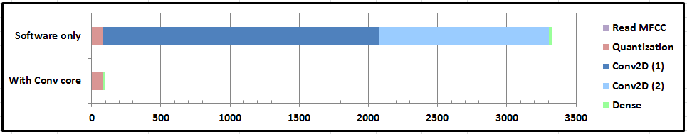
These measurements use a second timer peripheral on the SoC to get precise time elapsed in clock cycles. Each inference takes 89 ms to complete. This means 11.1 invoke / second, which is a good rate for detecting words in a 1 second timeframe:
Demo
Let’s test it for real:
Improvements
1. Input quantization
In term of performance, the bottleneck is now located in the input quantization step. This is slow because of the floating point division involved. Minerva does not support floating point operation so this is emulated in software with compiler-rt.
This could be done in FPGA with a dedicated core using the scales and zero points values from the model file.
2. Implement other layers
For now only the convolution layer is implemented in FPGA. Supporting more layer types in FPGA, especially the dense (fully connected) layer will improve the performance.
3. No software
In fact, once all the required layers for a given model are implemented in FPGA, there is no longer a need for software. In this case we could get rid of TensorFlow Lite Micro and have a FPGA-only solution, tailored for our model. In this case having a FPGA SoC is also not needed, we could remove Minerva CPU, LiteDRAM, Wishbone Bus, etc… which would make room for a bigger (and more accurate) model, where the layer cores are simply chained together via data streams.